Purpose
The RT4532 is a high-efficiency LED driver for backlight applications with an internal schottky diode and current source driver.
It supports linear mappings with 256 steps to setup the brightness of backlight LEDs. It also supports PWM dimming to adjust the brightness. This document explains the function and use of the RT4532 evaluation board (EVB) and provides information to enable operation and modification of the evaluation board and circuit to suit individual requirements.
Introduction
General Product Information
The RT4532 is a high-efficiency LED driver for backlight applications. An asynchronous boost converter with an internal Schottky diode and a current source driver are designed to support 6LED/channel with wide input voltage range from 2.5V to 5.5V.
This document explains the function and use of the RT4532 evaluation board (EVB) and provides information to enable operation and modification of the evaluation board and circuit to suit individual requirements.
Product Feature
- Input Voltage Range : 2.5V to 5.5V
- Internal Schottky Diode
- Fast-speed mode I2C Compatible Interface
- Drive Up to 6 WLEDs in 4 String
- External PWM Brightness Control
- 550k/1.1MHz Switching Frequency
- Built-in Internal Soft-Start
- I2C Programmable 256 Steps Linear Current Regulation
- Up to 85% Efficiency with Small Magnetics
- Programmable 16V/24V OVP
- Current Accuracy ±5% and Current Balance ±3%
- UVLO, OVP, OCP, OTP Protection
- Shutdown Current : < 1µA
- Temperature Range : -40°C to 85°C
Key Performance Summary Table
|
Key Features
|
Evaluation Board Number : PCB015_V1
|
|
Default Input Voltage
|
2.5V~5.5V
|
|
Max Output Current
|
20mA/40mA
|
|
Default Output Voltage
|
17V
|
|
Default Marking & Package Type
|
RT4532
|
|
Operation Frequency
|
Steady 1.1MHz at all loads
|
|
Protection
|
UVLO
OVP
OCP
Thermal Shutdown
|
Bench Test Setup Conditions
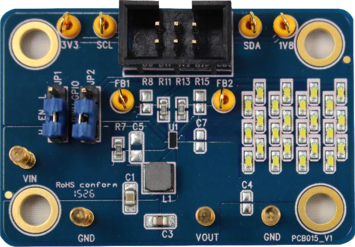
Headers Description and
Placement
Please carefully inspect the EVB IC and external components, comparing them to the following Bill of Materials, to ensure that all components are installed and undamaged. If any components are missing or damaged during transportation, please contact the distributor or send e-mail to evb_service@richtek.com.
Test Points
The EVB is provided with the test points and pin names listed in the table below.
|
Pin No.
|
Pin Name
|
Comment (expected waveforms or voltage levels on test points)
|
|
A2
|
GND
|
Ground. The exposed pad must be soldered to a large PCB and connected to GND for maximum thermal dissipation.
|
|
B1
|
VOUT
|
Power Output of the Asynchronous Boost Converter for Backlight LEDs.
Connect a 1μF or larger ceramic capacitor from VOUT to ground.
|
|
B2
|
VIN
|
Power Input. Connect this pin to the input power supply voltage.
Connect a 10μF or larger ceramic capacitor from the VIN to ground.
|
|
C1
|
PWM
|
PWM Dimming Input for Backlight LED.
|
|
C2
|
EN
|
Enable Control Input (Active High). The chip is in shutdown mode when the EN pin is low.
|
|
D1
|
SDA
|
I2C Serial Data Input/Output. An external pull-up resistor is required.
|
|
D2
|
SCL
|
I2C Serial Data Input/Output. An external pull-up resistor is required.
|
|
E1
|
FB2
|
Single Output 2 for Backlight LED.
|
|
E2
|
FB1
|
Single Output 1 for Backlight LED.
|
Power-up & Measurement Procedure
1. Apply 3.6V nominal input power supply (2.5V < VIN < 5.5V) to the VIN and GND terminals.
2. The EN voltage is pulled to logic high by internal circuit to enable operation. Drive EN high (>1.05V) to enable operation or low (<0.4V) to disable operation. Pull EN pin to High pin that make EN voltage equal to VIN.
3. There is a 2-pin header JP2 “EN” for enable control. To use a jumper at “H” option to tie EN test pin to input power VIN for enabling the device. Inversely, to use a jumper at “L” option to tie EN test pin and ground GND for disabling the device.
4. The JP4 is the I2C control pin that incloud SDA, SCL, GND pin, and it need to connect to Richtek WrenBoard when use the RT4532 I2C dimming.
5. The ILED setting supports I2C dimming and PWM dimming as below.
Output ILED Setting
1. Linear Brightness Dimming
The chip is built-in an I2C 8-bit resolution brightness control with maximum 20mA/40mA selection. Reg0x02 <3> corresponds to full-scale LED current control. Reg0x04 <7:0> sets 8bits resolution brightness dimming control.

Where
ILED, Full : the full-scale LED current set by Reg0x02 <3>.
Code : the 8bit brightness code Reg0x04 <7:0> programmed by I2C interface.
2. PWM Brightness Dimming
Besides programmable built-in I2C backlight LED current control, the RT4532 features a built-in PWM dimming current control by setting Reg0x02 <6> to 1, offering a linear current dimming by external clock source. In order to guarantee the PWM dimming resolution (7 bit at >15kHz application), recommending dimming frequency have to be operated at range of 400Hz to 20kHz.
3. LED Short Protection
LED short protection prevents abnormal connection to cause IC damage avoiding FB1/FB2 connecting power supply. And, If unbalanced LEDs series (cause FB1 or FB2 > 9.6V) is different between channel1 and channel2, IC will also occur LED short event. As LED short event occur more than deglitch time 2ms, IC will shut-down latch until IC is reset by EN pin.
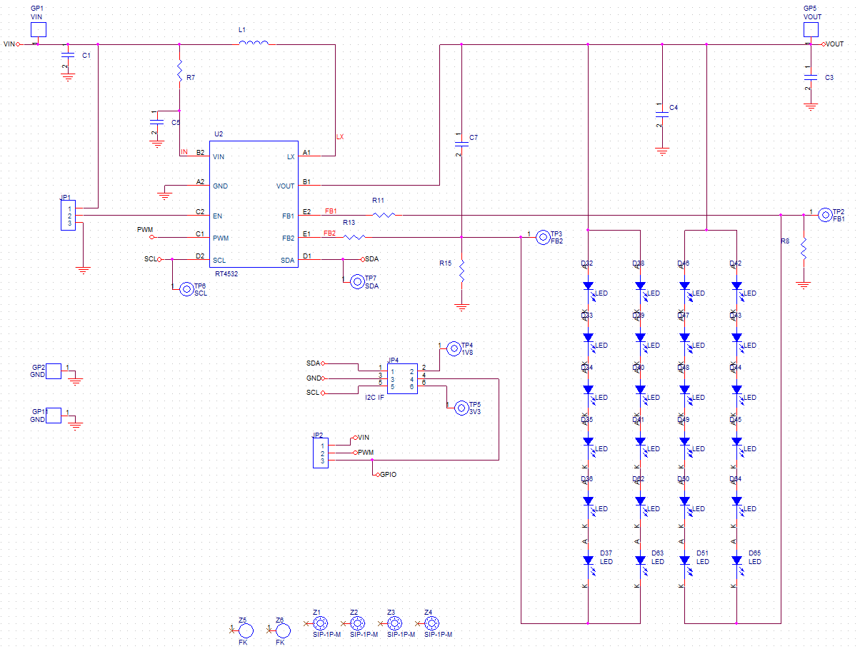
Schematic, Bill of Materials & Board Layout
EVB Schematic Diagram
Bill of Materials
|
Reference
|
Qty
|
Part Number
|
Description
|
Package
|
Manufacture
|
|
U2
|
1
|
RT4532
|
DC-DC Converter
|
CSP-10B 0.87x2.07
|
RICHTEK
|
|
L1
|
1
|
NR4018T100M
|
10µH/1.2A/±20%,
DCR = 0.18Ω, Inductor
|
4mm x 4mm x 1.8mm
|
TAIYO YUDEN
|
|
C1
|
1
|
0603X106M6R3
|
10µF/±20%/ 6.3V/X5R
Ceramic Capacitor
|
0603
|
Walsin
|
|
C3
|
1
|
C2012X7R1H105KT
|
1µF/±10%/50V/X7R
Ceramic Capacitor
|
0805
|
TDK
|
|
R7
|
1
|
|
Short
|
|
|
|
R11
|
1
|
|
Short
|
|
|
|
R13
|
1
|
|
Short
|
|
|
|
D32, D34, D36,
D33, D35, D37,
D38, D40, D62,
D39, D41, D63,
D46, D48, D50,
D47, D49, D51,
D42, D44, D64,
D43, D45, D65
|
24
|
|
LED
|
|
|
|
TP
|
6
|
3V3, SCL, SDA,
1V8, FB1, FB2
|
Test Pin
|
|
|
|
GP
|
4
|
VIN, GND, GND, VOUT
|
Golden Pin
|
|
|
|
JP
|
3
|
JP1, JP2, JP4
|
|
|
|
EVB Layout
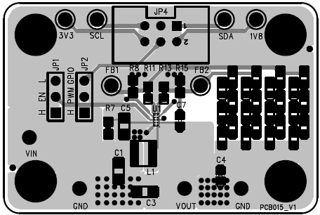
PCB Layout—Top View

PCB Layout—Bottom Side